- 您现在的位置:买卖IC网 > Sheet目录342 > MCBSTM32EXL (Keil)BOARD EVALUATION FOR STM32F103ZE
�� �
�
�RM0008�
�Advanced-control� timers� (TIM1&TIM8)�
�Bits� 2:0� SMS:� Slave� mode� selection�
�When� external� signals� are� selected� the� active� edge� of� the� trigger� signal� (TRGI)� is� linked� to�
�the� polarity� selected� on� the� external� input� (see� Input� Control� register� and� Control� Register�
�description.�
�000:� Slave� mode� disabled� -� if� CEN� =� ‘1’� then� the� prescaler� is� clocked� directly� by� the� internal�
�clock.�
�001:� Encoder� mode� 1� -� Counter� counts� up/down� on� TI2FP2� edge� depending� on� TI1FP1�
�level.�
�010:� Encoder� mode� 2� -� Counter� counts� up/down� on� TI1FP1� edge� depending� on� TI2FP2�
�level.�
�011:� Encoder� mode� 3� -� Counter� counts� up/down� on� both� TI1FP1� and� TI2FP2� edges�
�depending� on� the� level� of� the� other� input.�
�100:� Reset� Mode� -� Rising� edge� of� the� selected� trigger� input� (TRGI)� reinitializes� the� counter�
�and� generates� an� update� of� the� registers.�
�101:� Gated� Mode� -� The� counter� clock� is� enabled� when� the� trigger� input� (TRGI)� is� high.� The�
�counter� stops� (but� is� not� reset)� as� soon� as� the� trigger� becomes� low.� Both� start� and� stop� of�
�the� counter� are� controlled.�
�110:� Trigger� Mode� -� The� counter� starts� at� a� rising� edge� of� the� trigger� TRGI� (but� it� is� not�
�reset).� Only� the� start� of� the� counter� is� controlled.�
�111:� External� Clock� Mode� 1� -� Rising� edges� of� the� selected� trigger� (TRGI)� clock� the� counter.�
�Note:� The� gated� mode� must� not� be� used� if� TI1F_ED� is� selected� as� the� trigger� input�
�(TS=’100’).� Indeed,� TI1F_ED� outputs� 1� pulse� for� each� transition� on� TI1F,� whereas� the�
�gated� mode� checks� the� level� of� the� trigger� signal.�
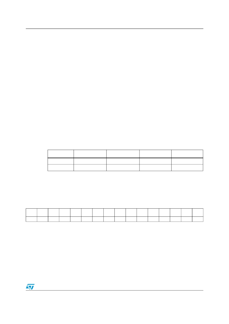
�Table� 72.�
�TIMx� Internal� trigger� connection� (1)�
�Slave� TIM�
�TIM1�
�TIM8�
�ITR0� (TS� =� 000)�
�TIM5�
�TIM1�
�ITR1� (TS� =� 001)�
�TIM2�
�TIM2�
�ITR2� (TS� =� 010)�
�TIM3�
�TIM4�
�ITR3� (TS� =� 011)�
�TIM4�
�TIM5�
�1.� When� a� timer� is� not� present� in� the� product,� the� corresponding� trigger� ITRx� is� not� available.�
�13.4.4�
�TIM1&TIM8� DMA/interrupt� enable� register� (TIMx_DIER)�
�Address� offset:� 0x0C�
�Reset� value:� 0x0000�
�15�
�Res.�
�Res.�
�14�
�TDE�
�rw�
�13�
�COMD�
�E�
�rw�
�12�
�CC4D�
�E�
�rw�
�11�
�CC3D�
�E�
�rw�
�10�
�CC2D�
�E�
�rw�
�9�
�CC1D�
�E�
�rw�
�8�
�UDE�
�rw�
�7�
�BIE�
�rw�
�6�
�TIE�
�rw�
�5�
�COMI�
�E�
�rw�
�4�
�CC4IE�
�rw�
�3�
�CC3IE�
�rw�
�2�
�CC2IE�
�rw�
�1�
�CC1IE�
�rw�
�0�
�UIE�
�rw�
�Bit� 15� Reserved,� always� read� as� 0.�
�Bit� 14� TDE� :� Trigger� DMA� request� enable�
�0:� Trigger� DMA� request� disabled.�
�1:� Trigger� DMA� request� enabled.�
�Bit� 13� COMDE� :� COM� DMA� request� enable�
�0:� COM� DMA� request� disabled.�
�1:� COM� DMA� request� enabled.�
�Doc� ID� 13902� Rev� 9�
�299/995�
�发布紧急采购,3分钟左右您将得到回复。
相关PDF资料
MCBTMPM330
BOARD EVAL TOSHIBA TMPM330 SER
MCIMX25WPDKJ
KIT DEVELOPMENT WINCE IMX25
MCIMX53-START-R
KIT DEVELOPMENT I.MX53
MCM69C432TQ20
IC CAM 1MB 50MHZ 100LQFP
MCP1401T-E/OT
IC MOSFET DRVR INV 500MA SOT23-5
MCP1403T-E/MF
IC MOSFET DRIVER 4.5A DUAL 8DFN
MCP1406-E/SN
IC MOSFET DVR 6A 8SOIC
MCP14628T-E/MF
IC MOSFET DVR 2A SYNC BUCK 8-DFN
相关代理商/技术参数
MCBSTM32EXLU
功能描述:开发板和工具包 - ARM EVAL BOARD + ULINK2 FOR STM32F103ZG
RoHS:否 制造商:Arduino 产品:Development Boards 工具用于评估:ATSAM3X8EA-AU 核心:ARM Cortex M3 接口类型:DAC, ICSP, JTAG, UART, USB 工作电源电压:3.3 V
MCBSTM32EXLU-ED
制造商:ARM Ltd 功能描述:KEIL STM STM32EXL EVAL BOARD
MCBSTM32EXLUME
功能描述:开发板和工具包 - ARM EVAL BOARD + ULINKME FOR STM32F103ZG
RoHS:否 制造商:Arduino 产品:Development Boards 工具用于评估:ATSAM3X8EA-AU 核心:ARM Cortex M3 接口类型:DAC, ICSP, JTAG, UART, USB 工作电源电压:3.3 V
MCBSTM32F200
功能描述:开发板和工具包 - ARM EVAL BOARD FOR STM STM32F207IG
RoHS:否 制造商:Arduino 产品:Development Boards 工具用于评估:ATSAM3X8EA-AU 核心:ARM Cortex M3 接口类型:DAC, ICSP, JTAG, UART, USB 工作电源电压:3.3 V
MCBSTM32F200U
功能描述:开发板和工具包 - ARM EVAL BOARD FOR STM STM32F207IG + ULINK2
RoHS:否 制造商:Arduino 产品:Development Boards 工具用于评估:ATSAM3X8EA-AU 核心:ARM Cortex M3 接口类型:DAC, ICSP, JTAG, UART, USB 工作电源电压:3.3 V
MCBSTM32F200UME
功能描述:开发板和工具包 - ARM EVAL BOARD FOR STM STM32F207IG ULINK-ME
RoHS:否 制造商:Arduino 产品:Development Boards 工具用于评估:ATSAM3X8EA-AU 核心:ARM Cortex M3 接口类型:DAC, ICSP, JTAG, UART, USB 工作电源电压:3.3 V
MCBSTM32F200UME-ED
制造商:ARM Ltd 功能描述:KEIL STM32F207IG EVAL BOARD
MCBSTM32F400
功能描述:开发板和工具包 - ARM EVAL BOARD FOR STM STM32F407IG
RoHS:否 制造商:Arduino 产品:Development Boards 工具用于评估:ATSAM3X8EA-AU 核心:ARM Cortex M3 接口类型:DAC, ICSP, JTAG, UART, USB 工作电源电压:3.3 V